
Tutorials

Introduction
This tutorial will teach you how to use an EDA (electronic design automation) software package called DipTrace to make your own circuit board. This tutorial will use a simple electrical continuity tester as the design, however a lot of what this tutorial provides goes directly into making any circuit board. There are any other EDA software packages available (KiCad, CadSoft EAGLE, Cadance OrCAD, Altium, etc.). Many of these programs are license based (you can only run the program on several computers which have been given a key). These licenses can be very expensive (~$10,000 for Altium). DipTrace has a free version, which is easy to use. I also recommend that you check out the need help section, where you'll find a ton of useful information.
DipTrace Basics
There are two major parts of DipTrace. One part, Schematic, is used to generate the schematic of a circuit design. The other major part, the PCB Layout, is used to design the actual physical printed circuit board (PCB) by placement of components and routing of traces.
There are also two additional modules within DipTrace; Pattern Editor and Component Editor. The pattern editor is used to create the actual physical part to be placed onto a PCB. These physical representations of components are called patterns (also sometimes referred to as “footprints”) and are stored in libraries for ease of access. Also, there are already-made pattern libraries, but you will create your own custom pattern library.
The component editor is used to create custom components represented as electrical symbols to be used in schematic designs. Once created these components are placed in libraries similar to patterns. There are a number of already-made component libraries that come with DipTrace, however you will learn how to create your own component library.
The general order of software use is first develop Pattern and Component libraries and design a schematic. Component libraries, either already-made or user-made, are used to accomplish this. Next, a physical representation of the schematic design developed is converted into physical components through a process which utilizes pattern libraries. After this conversion occurs, the layout editor is used to design the PCB; i.e., component placement and routing of interconnecting traces. This last step is often the most time consuming of all the steps. To accomplish the layout design while meeting all of the requirements specified in the list of requirements at the end of this document is a bit like a puzzle. There are an infinite number of acceptable solutions that meet the requirements, but the challenge is to accomplish this with efficiency by minimizing the overall lengths of traces while meeting all of the other design requirements.
Once the layout design is complete, the board design can be exported as art work and manufactured.
Pattern Editor
The pattern editor is used to create the pattern (physical dimension) of the component to be used in PCB Layout. To create a pattern the physical dimensions of the part is needed.
Key physical dimensions are:
- Component length, width or diameter
- Lead length
- Lead spacing
- Lead diameter
These dimensions can be obtained from component data sheets. If data sheets are not available, measuring by hand will suffice. For the optimum learning experience, you will create a pattern library for your continuity tester exercise with dimensions provided in this manual.
Component Editor
The component editor is similar to the pattern editor. However, the most important aspect of the component editor is the technique of attaching a pattern to a circuit symbol. This process is a key input into the conversion from your circuit design in Schematic (logical representation) into a physical representation of components in PCB Layout. If there is no library component for a part, it has to be made with use of the component editor. In your continuity tester exercise, you will make a component library from scratch
Schematic
This package of the software is used to enter the logical design of a circuit. Circuit symbols representing components should be placed as orderly as possible. After components have been placed, electrical connections, lines on the schematic, are inserted. Each component should have a reference designator (i.e., R1, R2, C1, U1 etc.) and a value (i.e., number of ohms for resistors, number of farads for capacitors, etc.) displayed.
When finished the entered schematic should look nearly identical to the original schematic.
PCB Layout
This software package is used to layout/design the final physical PCB, often it’s the most time consuming of all the steps. Once the schematic design is entered in Schematic, a conversion from a logical representation of components to a physical representation of components is accomplished through the use of patterns. After this conversion takes place, component placement and routing of traces can be accomplished. Layout has the capability to automatically placing components, as well as, automatically routing traces. However, there are limitations to these automatic features and often, when used, manual modification is necessary. Again, for the optimum learning experience, you will be expected to manually place components and manually route traces, so that your PCB design is unique.
Getting Started - Creating a Pattern Library for PCB Layout
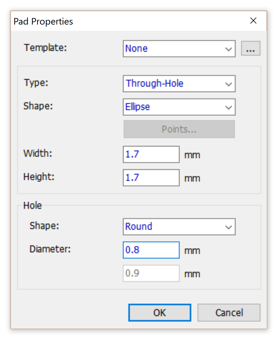 Before we jump into things, lets not complicate things more than they are. Since most the components share an identical pad size, lets set up a default pad size. Open up the pattern editor (make sure it's empty). Since most of what we are doing is in millimeters, go to view > Units and select mm. Now go to Pattern and select Default Pad Properties. Just as the image shows, the shape is an ellipse, the height and width of the pad is 1.7mm, the hole diameter is .8mm and through is selected. Now go to Library and select save. It will ask you for a name and hint, so just put MyLib in both (does nothing really). Save the file in a directory you can easily access. Name the file whatever you want, I chose MyLib as the file name. Now open the component editor and save a blank file just like we did in pattern editor, I named mine MyComp.
Now that you have been introduced to all four programs and properly set up, go to part 1 to get started. You can begin from any of the five components.